[LIS3LV02DL] 3축 가속도 센서 관련 자료
LIS3LV02DL은 디지털 인터페이스 SPI와 I2C를 선택 할 수 있는 3축 가속도 센서이다. 센서의 가동부는 MEMS 기술로 실리콘을 가공, 제작되었다. 회로 부분은 CMOS 기술로 제작 되었으며 고집적, 저소비전류이다. 또 센서의 특성에 맞춰 내부 트리밍되어 있어 고정밀도 센서 출력을 쉽게 얻을 수 있다.
LIS3LV02DL은 디지털 인터페이스 SPI와 I2C를 선택 할 수 있는 3축 가속도 센서이다. 센서의 가동부는 MEMS 기술로 실리콘을 가공, 제작되었다. 회로 부분은 CMOS 기술로 제작 되었으며 고집적, 저소비전류이다. 또 센서의 특성에 맞춰 내부 트리밍되어 있어 고정밀도 센서 출력을 쉽게 얻을 수 있다.
측정 가능한 가속도의 풀 스케일은 ±2g와 ±6g를 선택할 수 있고, 응답주파수는 640Hz로 고속이므로 폭넓은 분야에서 사용 할 수 있다.
특징
■ 2.16V TO 3.6V SINGLE SUPPLYOPERATION
■ 1.8V COMPATIBLE IOs
■ I2C/SPI DIGITAL OUTPUT INTERFACES
■ PROGRAMMABLE 12 or 16 BIT DATA REPRESENTATION
■ INTERRUPT ACTIVATED BY MOTION
■ PROGRAMMABLE INTERRUPT THRESHOLD
■ EMBEDDED SELF TEST
■ HIGH SHOCK SURVIVABILITY
■ ECO-PACK COMPLIANT
data sheet
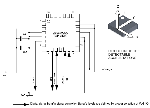
응용회로

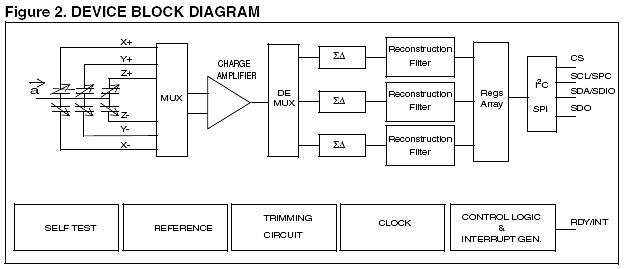
블록 다이어그램
센서부는 그림과 같이 콘덴서가 하프 브리지 상태로 되어 있다. 센서에 가속도가 가해지면 액추에이터가 이동하여 정전용량이 변화하고, 브리지가 비평형상태로 된다. 센서에 인가된 전압 펄스를 차지앰프로 적분하고, 정전용량의 변화를 출력한다. 센서의 정전용량은 평형 상태일 때 수pF, 최대 가속도가 가해졌을 때의 변화는 100pF 정도이다. 차지 앰프가 한 개이므로 센서부의 출력은 다중화(멀티플렉스)되지만 차지 앰프 출력은 역다중화(디멀티플렉스)되므로 각 축의 센서 출력을 독립적으로 얻을 수 있다. 차지 앰프의 클록은 61.5kHz이다.
센서로부터의 전압 출력은 3개의 ΔΣ 변환기(클록 주파수 20.5kHz)에 의해 비트 스트림으로 변환한다. 그 후 필터에서 디 지털 데이터로 변환하고 내부 레지스터에 저장한다. 이 데이터 는 SPI/I2C 인터페이스에 의해 마이컴에서 판독할 수 있다.
특징
■ 2.16V TO 3.6V SINGLE SUPPLYOPERATION
■ 1.8V COMPATIBLE IOs
■ I2C/SPI DIGITAL OUTPUT INTERFACES
■ PROGRAMMABLE 12 or 16 BIT DATA REPRESENTATION
■ INTERRUPT ACTIVATED BY MOTION
■ PROGRAMMABLE INTERRUPT THRESHOLD
■ EMBEDDED SELF TEST
■ HIGH SHOCK SURVIVABILITY
■ ECO-PACK COMPLIANT
data sheet
 invalid-file
응용회로
블록 다이어그램
센서부는 그림과 같이 콘덴서가 하프 브리지 상태로 되어 있다. 센서에 가속도가 가해지면 액추에이터가 이동하여 정전용량이 변화하고, 브리지가 비평형상태로 된다. 센서에 인가된 전압 펄스를 차지앰프로 적분하고, 정전용량의 변화를 출력한다. 센서의 정전용량은 평형 상태일 때 수pF, 최대 가속도가 가해졌을 때의 변화는 100pF 정도이다. 차지 앰프가 한 개이므로 센서부의 출력은 다중화(멀티플렉스)되지만 차지 앰프 출력은 역다중화(디멀티플렉스)되므로 각 축의 센서 출력을 독립적으로 얻을 수 있다. 차지 앰프의 클록은 61.5kHz이다.
센서로부터의 전압 출력은 3개의 ΔΣ 변환기(클록 주파수 20.5kHz)에 의해 비트 스트림으로 변환한다. 그 후 필터에서 디 지털 데이터로 변환하고 내부 레지스터에 저장한다. 이 데이터 는 SPI/I2C 인터페이스에 의해 마이컴에서 판독할 수 있다.
레지스터
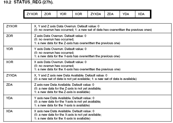
센서의 설정과 제어는 CTRL_REG1, 2, 3에서 실행한다. 각축의 가속도 측정 데이터의 상태값은 STATUS_REG를 이용한다.
주요 레지스터
CTL_REG1
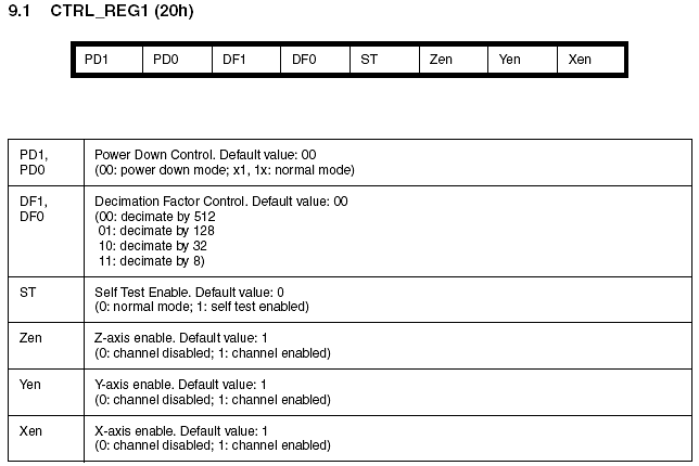
PD1, PD0 : 파워다운 모드 설정
PD1, PD0 = “00” -> 파워다운 모드 (default value after boot).
PD1, PD0 = "x1", "1x" -> 일반 동작 모드.
DF1,
DF0 : data rate(필터 설정으로 민감도를 설정할 수 있다. 높을수록 노이즈하지만 감도가 높아진다.)
default "00" data-rate = 40Hz. By changing the content of DF1,
“01”, “10” “11” ->160Hz, 640Hz, 2560Hz.
ST : self test function
0 : 일반 동작 모드, 1: self test모드
Zen : enables Z-axis (The default value is 1)
Yen : enables Y-axis (The default value is 1)
Xen : enables X-axis (The default value is 1)
-> 따라서 초기화시 1100 0111(0xC7)로 설정하면 정상동작 한다.
CTL_REG2
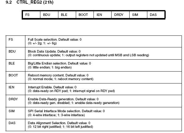
FS Scale 설정.
0 : +/-2g (default)
1 : +/-6g
BDU bit is used to inhibit output registers update until both upper and lower register parts are
read. In default mode (BDU= ‘0’) the output register values are updated continuously. If for any
reason it is not sure to read faster than output data rate it is recommended to set BDU bit to
‘1’. In this way the content of output registers is not updated until both MSB and LSB are read
avoiding to read values related to different sample time.
BLE Big Endian, Little Endian 설정
1 : Big Endian MSB->28h (X-axis), LSB ->29h (X-axis)
0 : Little Endian
BOOT bit is used to refresh the content of internal registers stored in the flash memory block.
At the device power up the content of the flash memory block is transferred to the internal registers
related to trimming functions to permit a good behavior of the device itself. If for any reason
the content of trimming registers was changed it is sufficient to use this bit to restore
correct values. When BOOT bit is set to ‘1’ the content of internal flash is copied inside corresponding
internal registers and it is used to calibrate the device. These values are factory
trimmed and they are different for every accelerometer. They permit a good behavior of the
device and normally they have not to be changed.
At the end of the boot process the BOOT bit is set again to ‘0’.
IEN bit is used to switch the value present on data-ready pad between Data-ready signal and
Interrupt signal. At power up the Data-ready signal is chosen. It is however necessary to modify
DRDY bit to enable Data-ready signal generation.
DRDY bit is used to enable DataReady pad activation. If DRDY bit is ‘0’ (default value) on DataReady
pad a ‘0’ value is present. If a DataReady signal is desired it is necessary to set to ‘1’
DRDY bit. DataReady signal goes to ‘1’ whenever a new data is available for all the enabled
axes. For example if Z-axis is disabled, DataReady signal goes to ‘1’ when new values are
available for both X and Y axes. DataReady signal comes back to ‘0’ when all the registers
containing values of the enabled axes are read. To be sure not to loose any data coming from
the accelerometer data registers must be read before a new DataReady rising edge is generated.
In this case DataReady signal will have the same frequency of the data rate chosen.
SIM SPI모드 설정
0 : (default value) the 4-wire interface
1 : 3-wire interface
DAS 12 bit, 16 bit 모드 설정, 최상의 비트는 부호비트 이다.
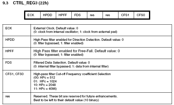
ECK bit selects whether the clock used in the core comes from internal oscillator or from external
pad OSC_IN. In the latter case internal oscillator is switched off and the pin Pull-Down
is disabled thus reducing power consumption. External clock must be in the range of 1.045
MHz +/- 10% and must have a duty cycle of 50%.
HPDD bit permits to select either filtered or not filtered data to feed the Signal Processing (Direction
Detection) block as described in Figure 10. When HPDD is set to ‘0’ (default mode) the
data used to generate DD interrupt come directly from digital block or temperature compensation
block while if HPDD is set to ‘1’ the interrupt signals are based on High-Pass filtered data.
For additional details about the data flow, please refer to Figure 10.
HPFF bit allows to select between filtered or not filtered data to be processed by the Signal
Processing (WakeUp or FreeFall) block as described in Figure 15. If HPFF is set ‘0’ (default
mode) data used to generate WU or FF interrupt come directly from digital block or temperature
compensation block while if HPFF is set ‘1’ the interrupt signals are based on High-Pass
filtered data. For additional details about the data flow, please refer to Figure 10.
FDS bit decides whether data stored in output registers are High Pass filtered or not. In default
mode (FDS bit set to ‘0’) signal are not filtered while it is possible to access data coming from
HP filter setting FDS bit to ‘1’. For additional details about the data flow, please refer to Figure
10.
CFS<1:0> bit select High-pass filter Cut-off Frequency coefficient. Increasing this number
makes Cut-off Frequency (@-3dB) move to lower values.
The Cut-off Frequency behavior is described by the following equation:
Where HPc = 512, 1024, 2048, 4096 when CFS<1:0>= 00, 01, 10, 11 respectively and ODR
represents the Output Data Rate selectable through the DF1, DF0 bits in CTRL_REG1.
The figure below gives a representation of the possible transfer functions obtained modifying
Output Data Rate and High Pass Filter coefficient (HPc).
가속도센서 출력 데이터
가속도 센서의 출력은 -2(6)g ~ +2(6)g까지 나오며 디지털 값으로 0~11비트(0~2047)까지 표현된다. 비트12 ~ 비트15는 부호를 나타낸다.
예로 1g라면 아래 표와 같이 0x0400(1024) 으로 출력되며, -1g라면 0xFC00 (-1024)로 출력된다.

SPI제어
CS핀이 0일 경우 SPI모드로 동작(1일 경우 I2C모드)
- Data Read
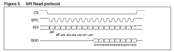
bit 0: READ bit. Read일경우 항상 1로 셋팅해야 함.
bit 1: MS bit. When 0 do not increment address, when 1 increment address in multiple reading.
bit 2-7: address AD(5:0). 레시스터의 주소 설정.
bit 8-15: data DO(7:0) (read mode). This is the data that will be read from the device (MSb
first).
bit 16-... : data DO(...-8). Further data in multiple byte reading.
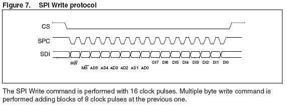
bit 0: WRITE bit. Write동작시 0으로 설정되어야 함.
bit 1: MS bit. When 0 do not increment address, when 1 increment address in multiple writing.
bit 2 -7: address AD(5:0). This is the address field of the indexed register.
bit 8-15: data DI(7:0) (write mode). This is the data that will be written inside the device (MSb
first).
bit 16-... : data DI(...-8). Further data in multiple byte writing.
센서의 설정과 제어는 CTRL_REG1, 2, 3에서 실행한다. 각축의 가속도 측정 데이터의 상태값은 STATUS_REG를 이용한다.
| 레지스터명 | Address | 초기값 | |
| WHO_AM_I | 0F | 111010 | 물리 어드레스=3Ah |
| OFFSET_X | 16 | 교정값 | X축의 오프셋 교정값 |
| OFFSET_Y | 17 | 교정값 | Y축의 오프셋 교정값 |
| OFFSET_Z | 18 | 교정값 | Z축의 오프셋 교정값 |
| GAIN_X | 19 | 교정값 | X축의 게인 교정값 |
| GAIN_Y | 1A | 교정값 | Y축의 게인 교정값 |
| GAIN_Z | 1B | 교정값 | Z축의 게인 교정값 |
| CTRL_REG1 | 20 | 111 | 필터의 계수와 각 축 동작의 가부, 셀프 테스트 ON/OFF 설정 등 |
| CTRL_REG2 | 21 | 0 | 풀 스케일 ±2g/±6g 선택, 출력 데이터 형식 선택 등 |
| CTRL_REG3 | 22 | 1000 | 방향 검지와 자유 낙하 등의 HPF 설정 등 |
| HP_FILTER RESET | 23 | 더미 | 판독에 따라 HP_FILTER를 리셋 |
| STATUS_REG | 27 | 0 | 각 축의 데이터 재기록 상태와 유효/무효 판단 |
| OUTX_L | 28 | 출력값 | X축의 가속도 데이터 (LSB) |
| OUTX_H | 29 | 출력값 | X축의 가속도 데이터 (MSB) |
| OUTY_L | 2A | 출력값 | Y축의 가속도 데이터 (LSB) |
| OUTY_H | 2B | 출력값 | Y축의 가속도 데이터 (MSB) |
| OUTZ_L | 2C | 출력값 | Z축의 가속도 데이터 (LSB) |
| OUTZ_H | 2D | 출력값 | Z축의 가속도 데이터 (MSB) |
| FF_WU_CFG | 30 | 0 | 인터럽트 설정용 |
| FF_WU_SRC | 31 | 0 | 인터럽트 플러그 |
| FF_WU_ACK | 32 | 더미 | 더미 레지스터 |
| FF_WU_THS_L | 34 | 0 | 자유 낙하 검지 임계값 (LSB) |
| FF_WU_THS_H | 35 | 0 | 자유 낙하 검지 임계값 (MSB) |
| FF_WU_DURATION | 36 | 0 | 자유 낙하/웨이크업 이벤트의 최소 주기 |
| DD_CFG | 38 | 0 | 인터럽트 설정용 |
| DD_SRC | 39 | 0 | 인터럽트 플러그 |
| DD_ACK | 3A | 더미 | 더미 레지스터 |
| DD_THSI_L | 3C | 0 | 방향 검지 임계값 (LSB) |
| DD_THSI_H | 3D | 0 | 방향 검지 임계값 (MSB) |
| DD_THSE_L | 3E | 0 | 방향 검지 외부 임계값 (LSB) |
| DD_THSE_H | 3F | 0 | 방향 검지 외부 임계값 (MSB) |
주요 레지스터
CTL_REG1
PD1, PD0 : 파워다운 모드 설정
PD1, PD0 = “00” -> 파워다운 모드 (default value after boot).
PD1, PD0 = "x1", "1x" -> 일반 동작 모드.
DF1,
DF0 : data rate(필터 설정으로 민감도를 설정할 수 있다. 높을수록 노이즈하지만 감도가 높아진다.)
default "00" data-rate = 40Hz. By changing the content of DF1,
“01”, “10” “11” ->160Hz, 640Hz, 2560Hz.
ST : self test function
0 : 일반 동작 모드, 1: self test모드
Zen : enables Z-axis (The default value is 1)
Yen : enables Y-axis (The default value is 1)
Xen : enables X-axis (The default value is 1)
-> 따라서 초기화시 1100 0111(0xC7)로 설정하면 정상동작 한다.
CTL_REG2
FS Scale 설정.
0 : +/-2g (default)
1 : +/-6g
BDU bit is used to inhibit output registers update until both upper and lower register parts are
read. In default mode (BDU= ‘0’) the output register values are updated continuously. If for any
reason it is not sure to read faster than output data rate it is recommended to set BDU bit to
‘1’. In this way the content of output registers is not updated until both MSB and LSB are read
avoiding to read values related to different sample time.
BLE Big Endian, Little Endian 설정
1 : Big Endian MSB->28h (X-axis), LSB ->29h (X-axis)
0 : Little Endian
BOOT bit is used to refresh the content of internal registers stored in the flash memory block.
At the device power up the content of the flash memory block is transferred to the internal registers
related to trimming functions to permit a good behavior of the device itself. If for any reason
the content of trimming registers was changed it is sufficient to use this bit to restore
correct values. When BOOT bit is set to ‘1’ the content of internal flash is copied inside corresponding
internal registers and it is used to calibrate the device. These values are factory
trimmed and they are different for every accelerometer. They permit a good behavior of the
device and normally they have not to be changed.
At the end of the boot process the BOOT bit is set again to ‘0’.
IEN bit is used to switch the value present on data-ready pad between Data-ready signal and
Interrupt signal. At power up the Data-ready signal is chosen. It is however necessary to modify
DRDY bit to enable Data-ready signal generation.
DRDY bit is used to enable DataReady pad activation. If DRDY bit is ‘0’ (default value) on DataReady
pad a ‘0’ value is present. If a DataReady signal is desired it is necessary to set to ‘1’
DRDY bit. DataReady signal goes to ‘1’ whenever a new data is available for all the enabled
axes. For example if Z-axis is disabled, DataReady signal goes to ‘1’ when new values are
available for both X and Y axes. DataReady signal comes back to ‘0’ when all the registers
containing values of the enabled axes are read. To be sure not to loose any data coming from
the accelerometer data registers must be read before a new DataReady rising edge is generated.
In this case DataReady signal will have the same frequency of the data rate chosen.
SIM SPI모드 설정
0 : (default value) the 4-wire interface
1 : 3-wire interface
DAS 12 bit, 16 bit 모드 설정, 최상의 비트는 부호비트 이다.
ECK bit selects whether the clock used in the core comes from internal oscillator or from external
pad OSC_IN. In the latter case internal oscillator is switched off and the pin Pull-Down
is disabled thus reducing power consumption. External clock must be in the range of 1.045
MHz +/- 10% and must have a duty cycle of 50%.
HPDD bit permits to select either filtered or not filtered data to feed the Signal Processing (Direction
Detection) block as described in Figure 10. When HPDD is set to ‘0’ (default mode) the
data used to generate DD interrupt come directly from digital block or temperature compensation
block while if HPDD is set to ‘1’ the interrupt signals are based on High-Pass filtered data.
For additional details about the data flow, please refer to Figure 10.
HPFF bit allows to select between filtered or not filtered data to be processed by the Signal
Processing (WakeUp or FreeFall) block as described in Figure 15. If HPFF is set ‘0’ (default
mode) data used to generate WU or FF interrupt come directly from digital block or temperature
compensation block while if HPFF is set ‘1’ the interrupt signals are based on High-Pass
filtered data. For additional details about the data flow, please refer to Figure 10.
FDS bit decides whether data stored in output registers are High Pass filtered or not. In default
mode (FDS bit set to ‘0’) signal are not filtered while it is possible to access data coming from
HP filter setting FDS bit to ‘1’. For additional details about the data flow, please refer to Figure
10.
CFS<1:0> bit select High-pass filter Cut-off Frequency coefficient. Increasing this number
makes Cut-off Frequency (@-3dB) move to lower values.
The Cut-off Frequency behavior is described by the following equation:
Where HPc = 512, 1024, 2048, 4096 when CFS<1:0>= 00, 01, 10, 11 respectively and ODR
represents the Output Data Rate selectable through the DF1, DF0 bits in CTRL_REG1.
The figure below gives a representation of the possible transfer functions obtained modifying
Output Data Rate and High Pass Filter coefficient (HPc).
가속도센서 출력 데이터
가속도 센서의 출력은 -2(6)g ~ +2(6)g까지 나오며 디지털 값으로 0~11비트(0~2047)까지 표현된다. 비트12 ~ 비트15는 부호를 나타낸다.
예로 1g라면 아래 표와 같이 0x0400(1024) 으로 출력되며, -1g라면 0xFC00 (-1024)로 출력된다.
SPI제어
CS핀이 0일 경우 SPI모드로 동작(1일 경우 I2C모드)
- Data Read
bit 0: READ bit. Read일경우 항상 1로 셋팅해야 함.
bit 1: MS bit. When 0 do not increment address, when 1 increment address in multiple reading.
bit 2-7: address AD(5:0). 레시스터의 주소 설정.
bit 8-15: data DO(7:0) (read mode). This is the data that will be read from the device (MSb
first).
bit 16-... : data DO(...-8). Further data in multiple byte reading.
bit 0: WRITE bit. Write동작시 0으로 설정되어야 함.
bit 1: MS bit. When 0 do not increment address, when 1 increment address in multiple writing.
bit 2 -7: address AD(5:0). This is the address field of the indexed register.
bit 8-15: data DI(7:0) (write mode). This is the data that will be written inside the device (MSb
first).
bit 16-... : data DI(...-8). Further data in multiple byte writing.
반응형

